In recent years, Fan-Out Panel-Level Packaging (FOPLP) has emerged as a prominent trend in semiconductor packaging technology. By embedding semiconductor chips directly into large-area panels for fan-out packaging, FOPLP achieves a higher integration level, improved electrical performance, and larger package sizes. Compared to traditional packaging methods, FOPLP enables higher I/O density, effectively enhancing production efficiency and reducing manufacturing costs.
Advantages of Mirle Group’s Solution
1. Extensive Panel Handling Experience
Mirle Group has extensive expertise in handling and storing various panel types, (300*300/510*515/600*600mm) including:
• Metal Carrier
• Glass Carrier
• Organic Core Substrate
• Glass Core Substrate
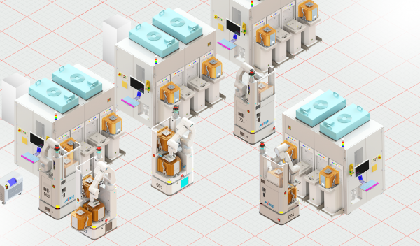
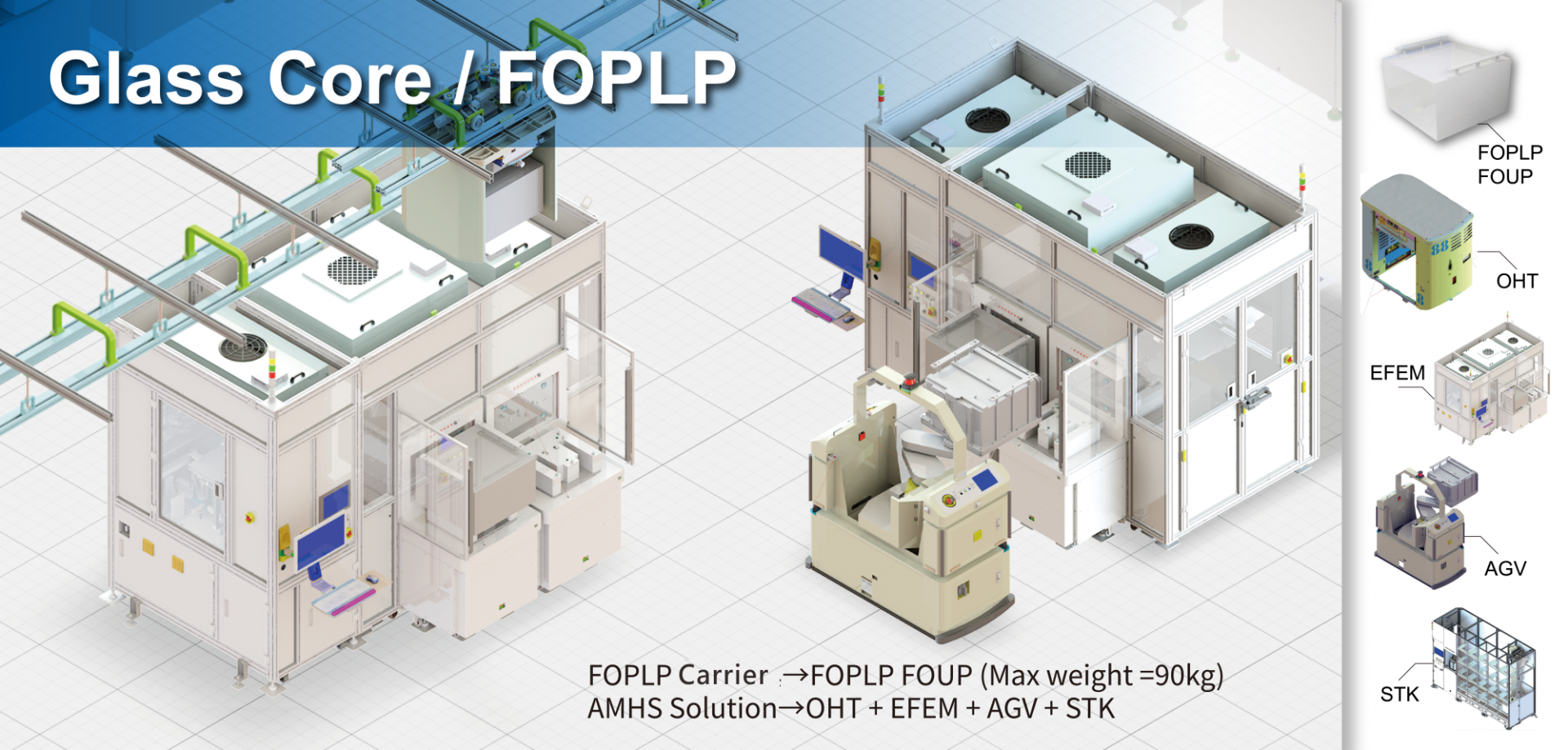
The company leverages in-house developed and manufactured products—including EFEM, STK, OHT, and AGV—to provide fully integrated automation solutions. This supports customers in achieving high levels of automation across all stages of advanced packaging processes.
2. Intelligent Manufacturing
Through precise equipment networking and real-time feedback, coupled with war-room-style logistical management, Mirle enhances data tracking and yield monitoring in FOPLP production lines. This capability is particularly critical for panel-level packaging technology.
3. Customized Solutions
Mirle complies with SEMI STANDARD E181/E182 while tailoring automated production equipment and systems to meet customer-specific needs. These solutions are designed to adapt to the unique product features and high-automation demands of various packaging manufacturers.
 Advantages of FOPLP
1. High Effective Integration
FOPLP utilizes large-area panels for packaging, maximizing space efficiency to accommodate and stack more chips. This approach enables both homogeneous and heterogeneous integration.
2. Cost Reduction
Panels offer a larger usable area compared to 300mm wafers. For instance, a panel can house 3–7 times the number of chips that a 300mm wafer can accommodate. This significantly improves production efficiency, minimizes material waste, and lowers costs.
3. Enhanced Transmission Efficiency
By reducing the distance between chips and external connections, FOPLP improves signal transmission speed and electrical performance. The superior chemical, physical, and optical properties of glass provide high reliability in conductivity and heat dissipation, making it particularly advantageous for homogeneous /heterogeneous integration and current CPO (Co-Packaged Optics) processes.
Fan-Out Panel-Level Packaging (FOPLP)
In recent years, Fan-Out Panel-Level Packaging (FOPLP) has emerged as a prominent trend in semiconductor packaging technology. By embedding semiconductor chips directly into large-area panels for fan-out packaging, FOPLP achieves a higher integration level, improved electrical performance, and larger package sizes. Compared to traditional packaging methods, FOPLP enables higher I/O density, effectively enhancing production efficiency and reducing manufacturing costs.
Advantages of Mirle Group’s Solution
1. Extensive Panel Handling Experience
Mirle Group has extensive expertise in handling and storing various panel types, (300*300/510*515/600*600mm) including:
• Metal Carrier
• Glass Carrier
• Organic Core Substrate
• Glass Core Substrate
The company leverages in-house developed and manufactured products—including EFEM, STK, OHT, and AGV—to provide fully integrated automation solutions. This supports customers in achieving high levels of automation across all stages of advanced packaging processes.
2. Intelligent Manufacturing
Through precise equipment networking and real-time feedback, coupled with war-room-style logistical management, Mirle enhances data tracking and yield monitoring in FOPLP production lines. This capability is particularly critical for panel-level packaging technology.
3. Customized Solutions
Mirle complies with SEMI STANDARD E181/E182 while tailoring automated production equipment and systems to meet customer-specific needs. These solutions are designed to adapt to the unique product features and high-automation demands of various packaging manufacturers.
Advantages of FOPLP
1. High Effective Integration
FOPLP utilizes large-area panels for packaging, maximizing space efficiency to accommodate and stack more chips. This approach enables both homogeneous and heterogeneous integration.
2. Cost Reduction
Panels offer a larger usable area compared to 300mm wafers. For instance, a panel can house 3–7 times the number of chips that a 300mm wafer can accommodate. This significantly improves production efficiency, minimizes material waste, and lowers costs.
3. Enhanced Transmission Efficiency
By reducing the distance between chips and external connections, FOPLP improves signal transmission speed and electrical performance. The superior chemical, physical, and optical properties of glass provide high reliability in conductivity and heat dissipation, making it particularly advantageous for homogeneous /heterogeneous integration and current CPO (Co-Packaged Optics) processes.